The Largest Chip Contract Ever Signed
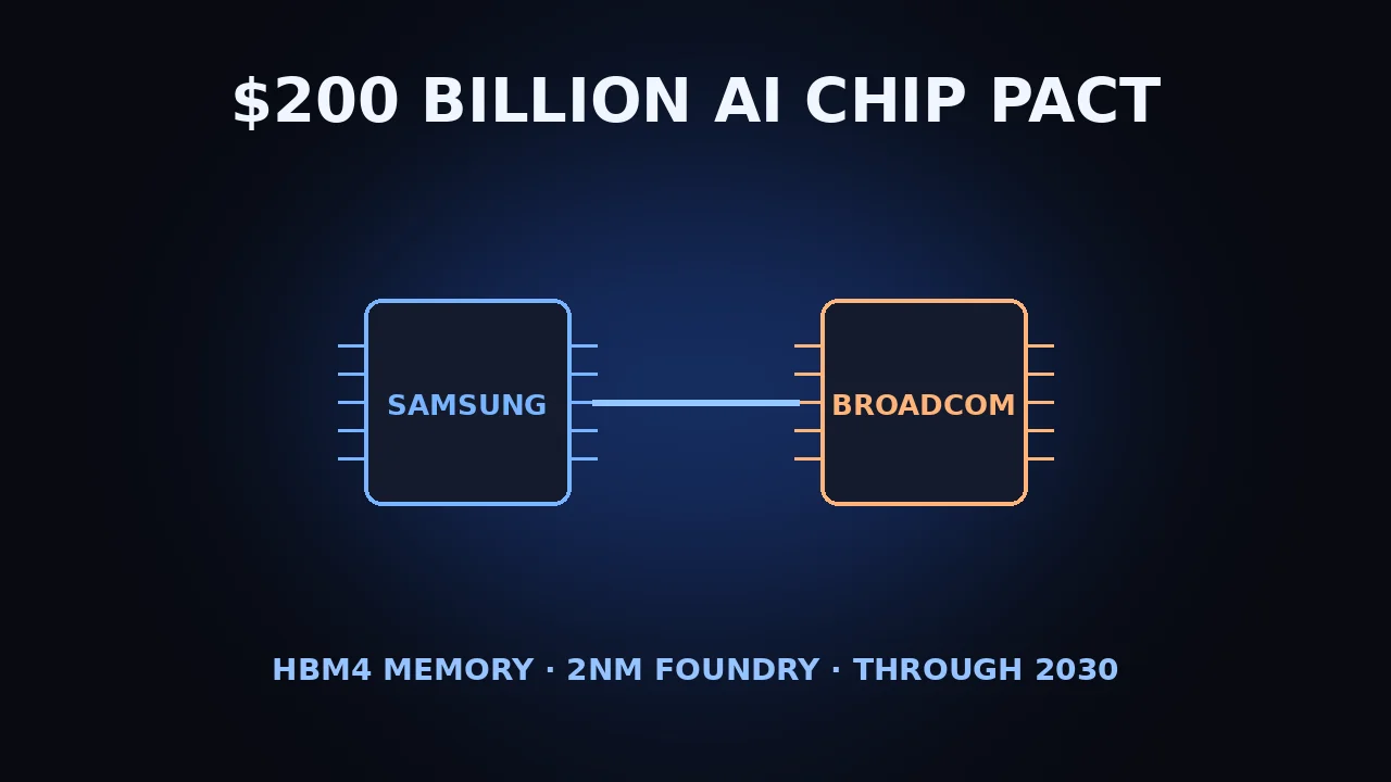
On July 24, 2026, Samsung Electronics and Broadcom signed an agreement covering up to $200 billion of AI semiconductor work through 2030. By value it is the largest semiconductor manufacturing contract on record, and it lands at the precise pressure point of the AI buildout: not the models, but the physical capacity to make the chips that run them.
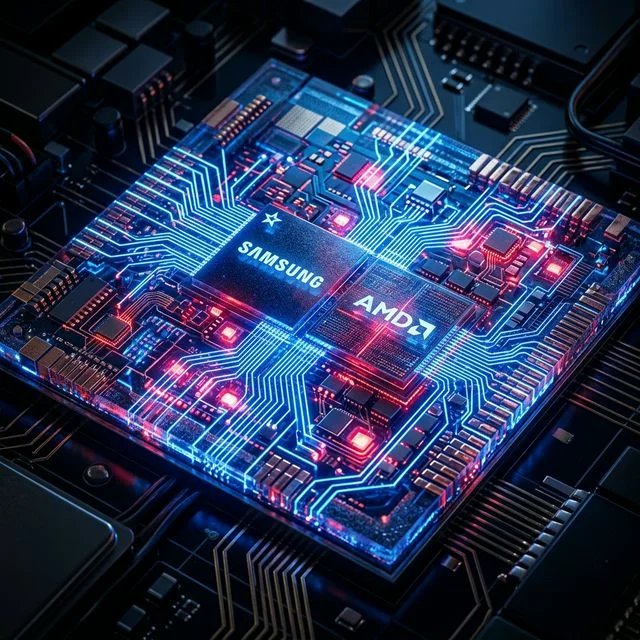
The scope is unusually broad. Samsung will manufacture Broadcom's next-generation AI accelerators and networking silicon on its 2-nanometre and below gate-all-around process nodes, and separately supply next-generation high-bandwidth memory — HBM4 and HBM4E — for those same accelerators. Memory, logic, and advanced packaging in one arrangement.
One caveat worth stating plainly: reporting indicates the agreement was signed as a memorandum of understanding. That makes it a strong statement of intent with an enormous headline number attached, not a fully binding purchase commitment. Deals of this scale typically convert into firm orders in stages.
Why Broadcom Needed This
Broadcom has quietly become one of the most important companies in AI infrastructure without designing a single consumer product. Its custom accelerators — built for hyperscalers who want alternatives to Nvidia's GPUs — and its networking silicon sit inside a large share of the world's AI data centres.
That business has been constrained by one thing: manufacturing capacity at the leading edge, where TSMC has been both the primary supplier and a bottleneck shared with Apple, Nvidia, AMD, and everyone else. Securing dedicated 2nm capacity plus the HBM to go with it removes Broadcom's single greatest supply risk through the end of the decade.
Why It Matters for Samsung — and TSMC
Samsung's foundry division has spent years as the credible second choice that could not quite convert scale customers, losing marquee accounts to TSMC's superior yields. An anchor customer of Broadcom's size at 2nm changes that trajectory: it validates the gate-all-around process commercially, funds the next capacity expansion, and gives Samsung a reference win to pitch to every other AI silicon designer.
For TSMC, this is the most serious competitive development in years. It does not lose its lead — TSMC's process advantage and customer roster remain formidable — but the industry's assumption that advanced AI silicon must be fabbed in Taiwan is now weaker than it was a week ago. Given the geopolitical concentration risk that assumption carries, a viable second source has strategic value beyond price.
The Memory Angle Is the Underrated Half
Most coverage leads with the foundry deal, but HBM may matter more. High-bandwidth memory has become the true constraint on AI accelerator performance — a modern chip's ceiling is often set by how fast it can be fed, not how fast it computes. HBM4 raises that ceiling substantially, and supply has been tight enough to shape product roadmaps across the industry.
Samsung supplying both the logic and the memory for the same accelerators means tighter co-design and fewer integration handoffs, which in this generation of hardware is a genuine performance lever rather than a procurement detail.
What to Watch
Three markers will show whether the headline number becomes real: conversion from MOU into firm multi-year orders; independent confirmation of Samsung's 2nm yield rates, which have been the historic obstacle; and whether other AI silicon designers follow Broadcom now that a second leading-edge supplier has a marquee reference.
The AI buildout's constraint has shifted from algorithms to atoms. This deal is what that shift looks like on a balance sheet.



























































Commenting is currently unavailable on this article.